
Probably about 12 years ago, I recovered the imaging sensor from an A4 flatbed scanner that had become obsolete. (I think its obsolescence was due to it having a parallel port interface and my family’s new computer didn’t have a parallel port) Apart from it not being able to communicate with a new computer, it still worked fine sadly. Fortunately, there were several useful components that I recovered from it including a stepper motor, v-belts and pulleys, CCFL light and the CCD.
Well, after all that time saying that one day I’ll get the CCD to work, the time has come.

There are several different circuits on this one PCB serving different functions. There, is the CCD itself; with all the logic signals to drive it, 12V supply and output amplifiers. Also, there is a switching boost converter to generate the high voltage to drive the CCFL light.
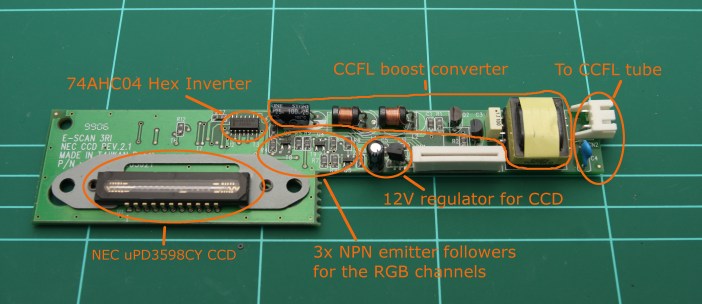
Something that has slowed me from getting started on this project has been I didn’t have any details on the CCD. There are no part numbers on the PCB or the side of the CCD, all I knew was that it was an NEC part, as printed on the PCB. To be able to interface to the CCD, I need to know pin functions. So, I took the plunge at removing the chip form the PCB.
If you’ve tried desoldering a DIP chip from a PCB using an iron, it can be difficult and can result in damage to the chip and PCB. I started using desoldering braid knowing that it may not work. And it didn’t, the solder had a very high melting temp (it is probably lead free solder) and the braid couldn’t soak up all the solder between the holes and pins. I had to resort to a more persuasive method – the hot air gun. Similarly, a hot air gun can damage components and I’ve noticed that the PCB usually appears heat affected. (I don’t have a proper de-soldering hot air station so I can’t comment on them not damaging the PCB)
Anyway, my hot air gun de-soldering method is straight-forward; hold the PCB upside down over the kitchen sink and apply even hot air to the soldered side of the PCB. Keep fingers clear of the hot air, and within a few seconds, the solder will melt and the components will fall off the PCB due to gravity. Remember to hold the PCB close to the sink so the components do bounce too far. Also, its a good idea to make sure there are no puddles of water in the sink. (I forgot to check when I de-soldered this board and the CCD bounced into some water. Hopefully it still works).


As suspected, the device number was on the back of the chip, it is a D3598CY manufactured by NEC during week 47 of 1998.
Searching for a datasheet for the device has been fruitless. There are plenty of suppliers of large quantities of this chip out of China (are these CCDs still being used?) but no datasheets. No details could be found from NEC, Renesis (I think they bought out NEC’s semiconductor division) or on any of the large datasheet websites.
Of the little data that I have found, I managed to find a 1997 NEC product catalogue detailing the chip’s specs:
- Full part number: μPD3598
- Pixels: 2700 x 3 (RGB)
- Pixel size: 8 x 8 μm
- Max data rate: 3 MHz
- Typical sensitivities
- Red: 11.1 V/lx·s
- Green: 12.5 V/lx·s
- Blue: 7.5 V/lx·s
- Features:
- High sensitivity
- Low noise
- Sample & Hold
- Clamp circuit
- 8-line spacing (64 mm)
- 3-output
I have managed to find some great information on how NEC CCDs work from NEC themselves (details to come). However, still no datasheet with the pin outs for the μPD3598 yet. Despite this, I traced out the PCB’s circuitry with a multimeter and transistor tester.
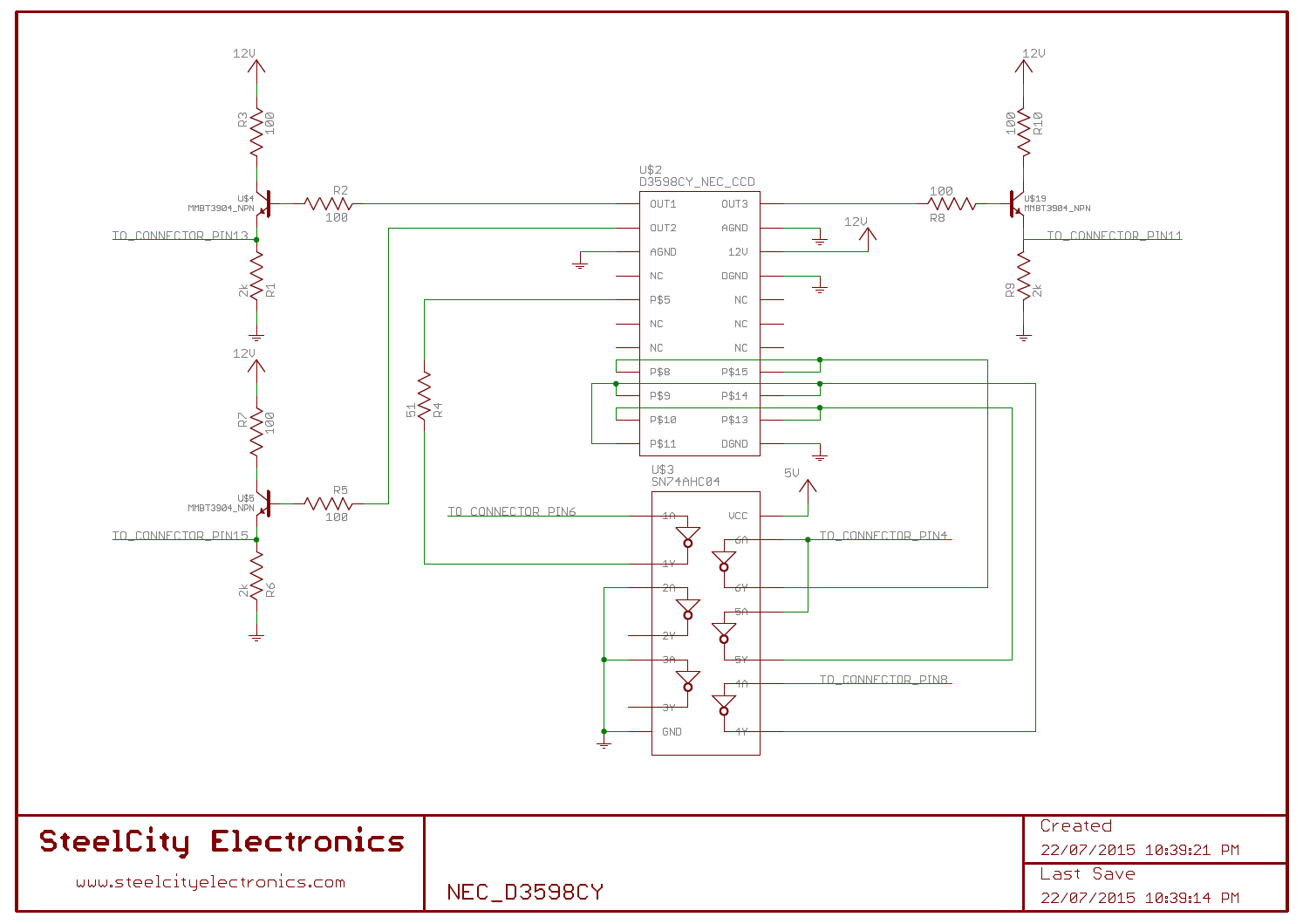
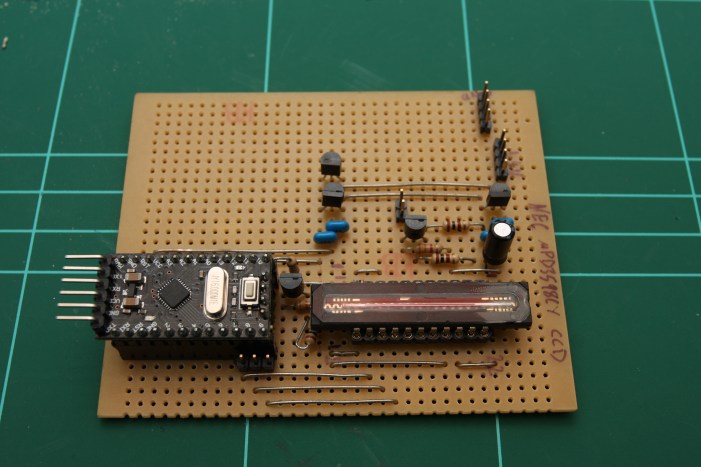
From this schematic and research into how linear CCDs operate, I have been able to make some very educated guesses at the functions of the pins. From this, I have built up a test bed that I’ll use to hopefully extract some data from the chip – provided that I didn’t kill it during de-soldering.
More details to come… but here is a sneak peek. Update: So I’ve finally started this project again, and I’m sort of getting a signal out of this thing.

Very interesting project! where you able to find the sensor’s datasheet? Yesterday I found a similar CCD and I was thinking to start a similar project. Thanks Miguel
LikeLike
Have you look at the upd3799cy datasheet?
LikeLike
Not sure about you circuit, but from the D3799CY that I hope is similar you need to drive signals with 5V and follow the timing of the datasheet.
I’m doing some experiments with the upD3597CY and an FPGA with a voltage adapter, no datasheet here too and to now I am guessing this pinout:
— OUT1 OUT3 —
— OUT2 AGND —
— AGND VOD —
— NC DGND —
— phiRB NC —
— NC NC —
— NC NC —
— phi2 phi2 —
— phiTG phiTG —
— phi1 phi1 —
— phiTG DGND —
I got the OUT signal moving according to the available light, so maybe I’m on the right track.
LikeLike