
Whats inside a power transistor? Well some semiconductor to be a transistor of course. How large would you expect the transistor’s die to be?
My guess is, that for a device that can conduct up to 10 A, the die would occupy the bulk of the transistor’s package. What’s your guess?
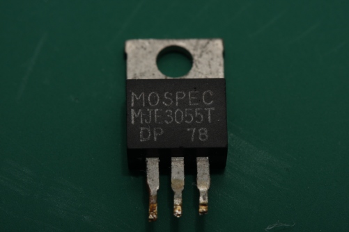
Lets find out with a teardown of sorts with the following MJE3055 NPN power transistor that comes in a TO-220 package.
With no access to an X-ray machine to photograph the device’s internals or even fuming nitric acid to de-cap the device, I had to look to other methods. My choice, brute force.
The brute force method is much more accessible to the masses. All you need is: a clamp, a needle file, some 180 grit sandpaper and a spare 1 hour.

Before we get too far, some quick specs on the MJE3055 NPN transistor:
- “…designed for use in general-purpose amplifier and switching applications”
- Maximum collector current (Ic) = 10A. – The maximum current (within limits) that device can conduct from collector to emitter.
- Maximum collector-Emitter voltage (Vceo) = 60Vdc. – The maximum voltage drop across the collector and emitter.
- Maximum power dissipation (Pd) = 75W.
The device’s pinout is shown next, note that the metal tab is also electrically connected to the Collector pin.

The dissection process was simple. Clamp the transistor in place using its metal tab and use a 5mm wide needle file to slowly remove the plastic packaging. This proved to be slow, so some 180 grit wet-and-dry sandpaper was wrapped around the file to increase the rate of plastic removal.
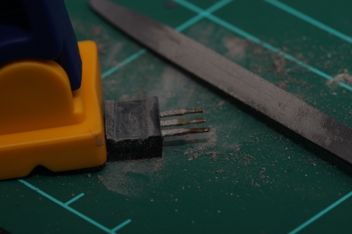
After some time (15 minutes?), not much had happened, probably 1-2mm of plastic removed.

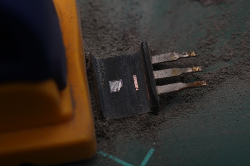
Back to filing and finally something. Two bond wires coming from the Base (bottom pin) and the Emitter (top pin) both going towards the centre of the device.

The bond wires are not very thick because all that remains are vertical sections of the bond wire. Their small diameter was not expected.

Next, the Base pin is exposed. The salmon colour is of the metal is certainly copper.

More filing to expose both the Base and Emitter pins within the device.

Finally, the Collector’s copper pin is revealed.

The Base and Emitter pins thickness has been filed through. Interestingly, the Collector pin bends down towards the metal case. Referring to the device’s pinout, the case and centre pin are both joined.

The bond wires become thicker and an outline to the left of the bond wires emerges. Could this be the die?

The rate of filing now slowed.
A closeup shot of the die. The filing has scratched the top left of the die, but the centre reveals a pattern of interlocking fingers. Also, what also appears to be weld spots for the bond wires in the centre of the die can be seen.

A bit more filing has exposed the perimeter of the die, but almost all of the die’s surface detail has been scratched off unfortunately.

I decided to stop at this point otherwise the whole die would be removed. Using some calipers, the die was measured to be about 1.8 mm x 1.8 mm. A very rough guess at the thickness of the die was made to be 0.25 mm thick. The total thickness of the remaining material (1.7 mm) minus the metal tab thickness (1.45 mm) gives a value of 0.25 mm.
Surprisingly, the transistor die was smaller than I expected – I assumed that the transistor semiconductor would occupy the bulk of the package. What was also unexpected was the fine gauge of the bond wires, particularly the emitter bond wire which can conduct up to 10 A.
For record’s sake, all of the spent sandpaper and the needle file that was used.


Try with a metallic 2n3055 🙂
LikeLike
I’ll see what I can do.
LikeLike
You’d be surprised how much current those bond wires can handle, as long as they’re short: I’ve found that 0.025 mm gold wires can handle more than 2 A continuously for a few days. From a quick image measurement, those look like about 0.15 mm diameter bond wires, probably made of aluminum: that’s 36 times more cross-sectional area, with only a little lower conductivity, so 10 A seems reasonable with a good heatsink, as far as the bond wires are concerned.
Incidentally, I’m a Ph. D. student studying wire bonding, and one of my projects has been investigating how much current the wire bonds can withstand, so I felt I should comment. 😛
LikeLiked by 1 person
Wow. Thanks for sharing your info Mike.
Will we ever see graphene be used for bond wires? I understand it has a resistivity even lower than silver.
Good luck with the PhD.
LikeLike
Funny, I also dabbled in graphene research for my master’s degree, but from a theoretical physics point of view, so I don’t know a lot about the practicalities of working with it. With that said, here’s my two cents.
Graphene bond wires seem unlikely to me, at least with anything like the process we use today for metal wires. It’s more than 10000 times thinner than the bond wires used today, so it’s likely too flexible without a thicker substrate that would take away the resistivity advantage. A resistivity advantage alone doesn’t motivate the industry that much, anyways, demonstrated by the fact that there hasn’t been much research into using pure silver wires: gold, copper, and aluminum are far more common, with some work recently on silver alloys that have higher resistivity than copper. Graphene also doesn’t bond easily to metals, from what I’ve read. Maybe graphene-graphene bonding could work; I haven’t found any research pointing one way or the other on that.
Graphene-based transistors or graphene interconnects on ordinary semiconductor dies seem like better places to start, then maybe with advances in high volume production techniques, we could look at ways to make longer interconnections that would replace metal bond wires.
LikeLike